Search
CLOSELaser micro/nanostructuring for smart surfaces, photonic and optoelectronic applications
Dr. Maria Kandyla
Laser structuring and functionalization of materials and devices
- Laser micro/nanostructuring for smart surfaces, photonic and optoelectronic applications
- Development and applications of nanocomposite thin films
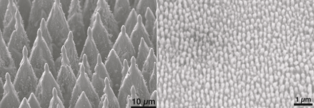
Irradiation of silicon by a big number of laser pulses in a liquid or gas environment creates quasi-periodic nanostructures or microstructures on the surface of the material, depending on the irradiation conditions and the surrounding medium. This method relies on single-step, maskless, tabletop laser processing of silicon, which is amenable to large-scale fabrication. Due to the unique electrical, optical, and mechanical properties of the laser-processed areas, microstructured and nanostructured silicon finds applications in the fabrication of optoelectronic devices, smart surfaces with controllable wettability, as well as a plasmonic substrate for SERS spectroscopy and optical trapping.
Large surface area applications
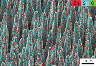
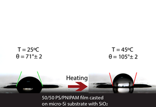
We combine laser-micro/nanostructured silicon substrates with thin layers of semiconducting materials, such as ZnO, to form semiconducting heterojunctions with a large surface area, to be used as photodetectors. Laser-microstructured ZnO/p-Si photodetectors demonstrate high sensitivity and broadband operation across the UV-Vis-NIR because they combine the optical properties of ZnO with the NIR absorbance of laser-processed silicon. Our fabrication method is scalable and versatile, does not require additional insulating layers, and can be extended to other combinations of materials. Combining microstructured silicon with thermoresponsive polymers, such as PNIPAM, or photoresponsive nanostructures, such as ZnO nanorods, we develop smart surfaces with a switchable wetting behavior. We can render the surfaces hydrophilic or hydrophobic by the use of external stimuli, such as temperature or light, for applications such as waterproof textiles, self-cleaning surfaces, microfluidics, and others.
Plasmonics
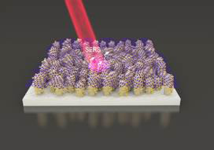
We develop highly efficient plasmonic optical tweezers, based on laser-structured silicon samples. Coating the samples with a thin layer of gold or silver results in the spontaneous formation of metallic nanoparticles on the surface. Using the gold/silver-coated nanostructured silicon samples as substrates for plasmonic optical trapping, we observe one order of magnitude enhancement in the trapping force, compared with conventional tweezers, for a broad range of trapping wavelengths. Integrating graphene with arrays of silicon nanopillars, decorated with gold nanoparticles, we observe broadband enhancement (2-3 orders of magnitude) in the Raman spectral signal across the entire visible electromagnetic spectrum. Conformation of graphene to the Au-decorated silicon nanopillars enables graphene to sample near fields from an increased number of nanoparticles. 2D materials present the unique ability of being easily combined with 3D substrates, as they can be grown over large areas with low-cost methods such as chemical vapor deposition, unlike bulk semiconductors which require high-quality epitaxial growth.
Key Publications
Laser structuring and functionalization of materials and devices
- Laser micro/nanostructuring for smart surfaces, photonic and optoelectronic applications
- Development and applications of nanocomposite thin films