Search
CLOSEPlanar Optical Components & Multifunctional Integrated Optical Circuits
Dr. Christos Riziotis
Applied Photonics – Materials & Devices
- Development of Photonic Sensors & Monitoring Systems
- Engineering of Plasmonic and Non-Linear Photonic Devices
- Planar Optical Components & Multifunctional Integrated Optical Circuits
- Photonic Engineering for Biomedical Applications
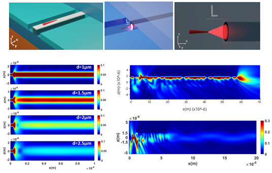
This activity is focusing on the design, analysis and fabrication of planar optical components as well as on waveguide and Bragg grating based integrated optical circuits and devices Analysis and modeling of waveguide-based components is performed by analytical accurate techniques like Couple Mode Theory or Normal Mode Analysis methods, while for rigorous modeling, techniques like FEM (Finite Element Method) or FDTD (Finite Difference Time Domain) are employed. Variational optimization and computational intelligent optimization techniques have been employed for design optimization of various devices.
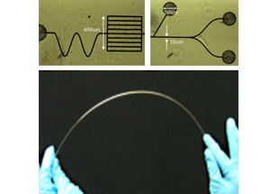
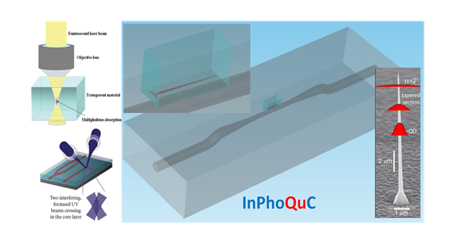
Fabrication of optical components and circuits are implemented by direct Laser writing techniques, (by femtosecond Laser, UV laser, or other sources) providing great flexibility for customization and rapid prototyping fabrication. Micro and nano-structures on various materials (Silica, Silicon, Semiconductors) can be fabricates by means of lased based writing. The group has also prior experience on the study and implementation of waveguides and optical components in different material systems, like Ga:La:S, oxide glasses, polymers, Lithium Niobate with various potential functionalities that can lead to applications like lasers development, electrooptic devices, nonlinear resonators etc.
A number of active and ongoing research collaborations have led to date to various implementations of such optical components with anticipated important applications in telecommunications, sensors, lab-on-chip, biomedical devices and hybrid quantum circuits.
A. Novel Integrated Optical Platforms for Enhanced Functionality
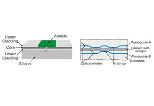
Novel techniques for waveguide and Bragg Grating inscription in Silica on Silicon platform have led to robust photonic integrated sensors for a range of chemical measurands. Exploitation of novel optical platforms such as the “Flat Fibre” platform has lead to the demonstration of waveguide components (ring and disk resonators, Mach Zehnder Interferometers, Bragg gratings etc) combined with the functionality of inscribed microfluidic channels has demonstrated the potential for the development of lab on chip devices for a variety of applications, like point of care diagnostics.
Key Publications
B. Hybrid Integrated Photonic Circuits for Quantum Applications
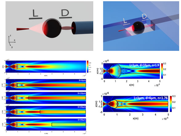
It has been proven theoretically that Quantum Computers can be implemented by combining and using classical optical gates and optical components, like, beam splitters, phase shifters, single photon sources and single photon detectors. Such Linear Optics Quantum Computers (LOQC) could be implemented by integrated photonics. In the frame of the project InPhoQuC the group is working towards the development of such quantum devices by the robust and highly controllable classical-in-nature integrated optical circuits based on Silica-on-Silicon material systems, which is the major integration platform compatible for interconnection with conventional optical fibers’ telecommunications infrastructure. Laser direct writing and micro-machining technology by infrared femtosecond laser and CW Ultraviolet Lasers are employing for the inscription of multifunctional waveguide structures and circuits. Integration of Nanowire Quantum Dots as quantum emitters, in silica based optical circuits has been enabled lately by a novel technique. Use of properly designed mirco-optical light focussing systems with the use of photonic nanojet generated by suitable high refractive index microspheres has led to record results with light coupling performance higher than 60%. This patented technique and advancement is anticipated to enable multiple quantum emitting functionality and scalable operation in hybrid circuits in various platforms, for quantum computing and sensing applications.
Key Publications
C. Riziotis, "LIGHT COUPLING BETWEEN NANOWIRE AND OPTICAL WAVEGUIDE BY MICROSPHERE PHOTONIC NANOJET",
European Patent Office. Patent Application, EP23386114.5 (09-11-2023).
International PCT Application PCT/EP2024/060953 (22-04-2024)
Applied Photonics – Materials & Devices
- Development of Photonic Sensors & Monitoring Systems
- Engineering of Plasmonic and Non-Linear Photonic Devices
- Planar Optical Components & Multifunctional Integrated Optical Circuits
- Photonic Engineering for Biomedical Applications