THEORETICAL & PHYSICAL CHEMISTRY INSTITUTE
 
  Infrastructure
  Materials Synthesis, Growth & Processing
  Materials & Devices Characterization Platforms
  Theoretical and Computational Chemistry and Materials Science
  Photonics and Νanostructures using short wavelength radiation
  Clean room for photonics applications and devices

Infrastructure - Photonics for Nano-applications

Photonics and Nanostructures using short wavelength radiation


Photonic Micro-machining of Surfaces and Photonic Synthesis of Nano-particles

Vacuum Ultra-violet (VUV)-micromachining workstation

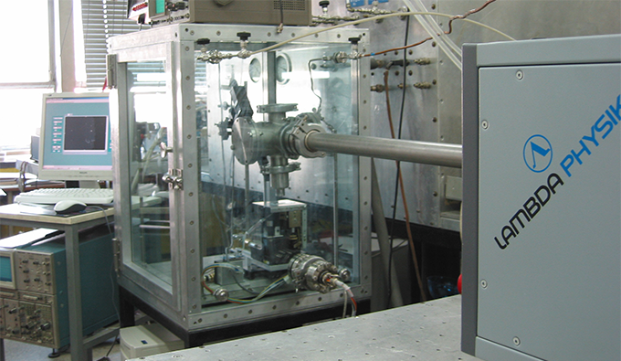
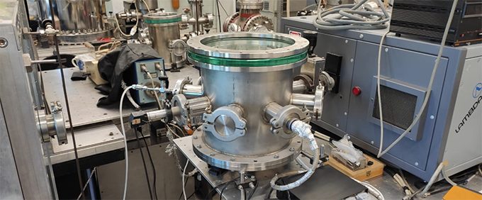
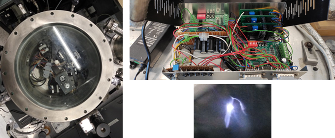
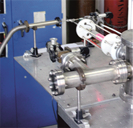
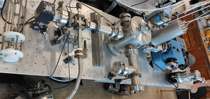
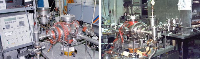
Vacuum Ultra-violet (VUV)-micromachining workstation, capable of processing different materials (from polymers to hard alloys) with ~2 μm resolution. A user-friendly software, (besides controlling the experimental parameters), has one additional degree of freedom that allows surface modification and processing with specified patterning.

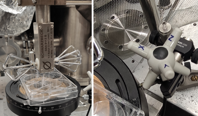
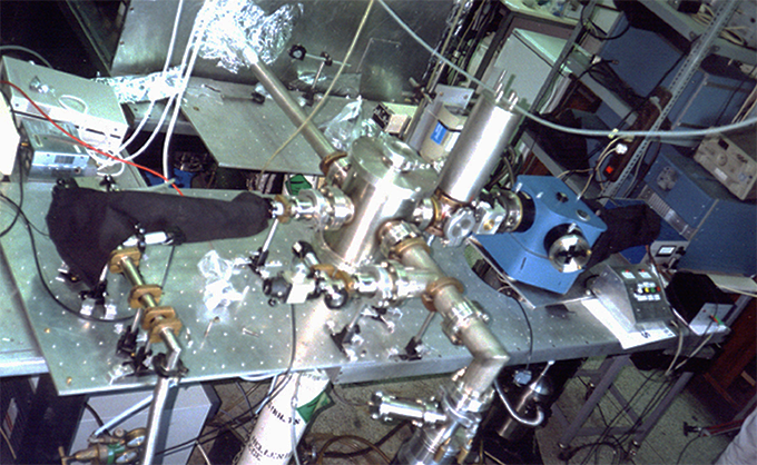
The main components of the system are: (1) The 157 nm molecular fluorine laser (by Lambda-Physik LPF 200). (2)  The VUV high quality beam projection optics. (3) The computer-controlled lab-made X-Y-Z-θ motorized stage, combined with one CCD imaging system for real time imaging and automatic control. The system is operating inside a glass chamber in N2 environment for surface processing and structure patterning. Applications include surface modification and functionalization of thin polymeric films for sensing and space applications and DNA chip manufacturing.

article image


VUV pulsed laser deposition workstation

VUV pulsed laser deposition workstation, used to fabricate core–shell nanostructures (1-100nm) of hard intermetallic alloys. The main components of the system are: (1) The 157 nm laser (by Lambda-Physik LPF 200). (2)  The VUV high quality axial laser beam focusing optics. (3) The computer-controlled X-Y-Z motorized stage bearing the substrate where the core-shells are grown. The system is operating at high vacuum conditions inside an all-stainless-steel chamber. Various nano-structured core-shells, semiconductors and quazicrystals, have been synthesized with this configuration. Applications include: (1) Investigation of the magnetic and electronic properties on nano-structures. (2) Development of new photonics systems with defined functionalization such as photovoltaics. (3) Hydrogen storage nano-materials from intermetallic alloys. (4) Quazicrystals, and (5) magnetic core-shells.

article image

article image


Imaging at the micro/nano-scale

Optical microscopes (Leica DMRX & Zeiss primovert)

Optical microscopes (Leica DMRX & Zeiss primovert)
Metallographic and inverted transmitted light microscopes for high resolution optical imaging of cells and materials. The microscopes are equipped with microscope cameras (PROGRES GRYPHAX) and image analysis software, operated at polarized and phase contrast modes. The Leica DMRX microscope can be combined with a thin-film-thickness measuring spectroscopic reflectrometer.

article image

Thin-film-measurement spectroscopic reflectometer (NanoCalc 2000)

Thin-film-measurement spectroscopic reflectometer (NanoCalc 2000)
Capable for thickness measurements from 10 nm up to 250 μm (400 μm).

Can be combined with the Leica DMRX optical microscope.

article image

Macro-lensing imaging system

Macro-lensing imaging system
Equipped with CCD cameras for real time surface imaging at long working distances with micrometric resolution, during photonic processing.

article image

Atomic (AFM) and Magnetic (MFM) Force Microscope (Quesant, Q-Scope™ 250)

Atomic (AFM) and Magnetic (MFM) Force Microscope (Quesant, Q-Scope™ 250)
Equipped with a 40-μm Dual PZT scanner. The available scanning modes are Contact AFM-Z Height and Lateral Force, Intermittent Contact AFM (Wave Modeª) and Phase Mode. 

The Q-Scope™ 250 is operating inside an acoustic and thermal isolation chamber and the stability of the system is controlled with a laser interferometer.

article image

Scanning Probe Microscopy (SPM) (Veeco di-Innova)

Scanning Probe Microscopy (SPM) (Veeco di-Innova)
Provides high resolution scanning, and a wide range of functionalities for physical chemistry and materials science. Offers a full suite of SPM techniques providing sample surface characterization both in air and liquid, such as:
Contact Mode; Tapping Mode; Lateral Force Microscopy (LFM); Scanning Tunnelling Microscopy (STM); Magnetic Force Microscopy (MFM); Phase Imaging; Conductive Atomic Force Microscopy (C-AFM); Scanning Thermal Microscopy (SThM); Force Distance Spectroscopy. Includes Nano-indentation capability.
A closed-loop scanner (80 x80 μm2 and Z > 7.5 μm) or an open-loop scanner (5 x 5 μm2 and Z > 1.5 μm) are available.

The SPM system is placed on a vibration isolation table (K-Minus Technology). The system   can operate as a nano-lithographic tool with 1 nm resolution. Combined with the VUV micro-machining apparatus it can achieve sub nano-meter resolution etching in the Z direction.

article image


Photon sources

X-UV and VUV light sources

X-UV light sources (30-110 nm) (cut-off wavelength of LiF window). These are stabilized discharge tubes of open geometry, which operate under differential vacuum pumping configurations.

VUV-light sources, which are coherent light sources (157 nm Laser) and incoherent light sources of stabilized discharge tubes of closed geometry operating over a wide spectral range.

article image

Lambda-Physik LPF 200 molecular fluorine (F2) laser

Lambda-Physik LPF 200 molecular fluorine (F2) laser emitting at 157nm. The pulse duration is 15 ns at full width at half maximum (FWHM). The maximum repetition rate and output energy are 20 Hz and 55 mJ, respectively. Capability of working at 193nm with the appropriate optics.

EKSPLA PL2250 ps-laser

EKSPLA PL2250 ps-laser emitting at 1064 nm, 532 nm and 266 nm. Pulse duration 30 ps at FWHM. Energy per pulse at repetition rate of 10Hz: 34 mJ at 1064 nm, 17 mJ at 532 nm and 3mJ at 266 nm. The system is equipped with an X-Y-Z micro-translator, beam analysis instrumentation (Tektronix oscilloscopes (7904), ps-photodiodes, energy meters, software and beam delivery system.


Emission and Detection of Microwave Radiation

Microwave emission and detection system for bio applications

Microwave emission and detection system for bio applications operated in a wide range of frequencies for measuring materials spectra and response in the microwave spectral range from 9 kHz to 3.3 GHz.

The system has mHz resolution capabilities and a precisely leveled, broad output power range with a front panel display. Excellent signal quality with low phase noise, good harmonic suppression and low spurious noise. The system supports AM/FM/PM and pulse modulation and has an internal low-drift OCXO reference.

article image


Simulator for space conditions

Ultra-high vacuum chamber for simulating space conditions

article image

The apparatus is an ultra-high vacuum (10-7 mbar) 316 stainless-steel chamber with capability of working at variable temperature (Janis 22C/350C, (8 - 475 K) and simultaneous irradiation by light sources, with controllable photon fluxes at selected VUV and X-UV wavelengths.

Applications include irradiation of biological samples in vivo to test survival rate in space or accelerating aging of satellite materials and adhesion and diffusion between interfaces of space surfaces.


Short wavelength light spectrometers

VUV absorption spectrometer and X-UV reflectometer

VUV absorption spectrometer and X-UV reflectometer
The absorption spectrometer operates over the spectral range from 110 to 200 nm. It consists of a lab-made hydrogen lamp operating in a longitudinal stabilized discharge mode, a stainless steel vacuum chamber and a VUV monochromator (by Acton, VM502) equipped with a solar-blind photomultiplier (EM1 9412).  It is also equipped with liquid nitrogen and a closed cycle helium cryogenic facility (by CTI-Cryogenic) for measurements at low temperatures (8-475 K). The high signal-to-noise ratio allows high-accuracy absorption coefficients measurements in thin polymeric films and optical materials. This set up can be operated as an X-UV reflectometer at the wavelength limit of 30 nm after differential pumping, which is well below the edge of the LIF window (110 nm).

article image

VUV mass spectroscopy

VUV mass spectroscopy
This workstation consists of a molecular beam apparatus, a quadrupole mass spectrometer (by Balzers, QMG 311) which can be operated on a “time of flight” mode if required, an F2 laser at 157 nm, and a data acquisition system.
The Balzers QMG 311 quadrupole mass spectrometer is a high-resolution apparatus, able to cover the 0–300 a.m.u. range.  The system consists of the control unit, the analyzer and the detection electronics. The analyzer is equipped with an electron impact ionization source in an open design and the detector is an off axis Secondary Electron Multiplier (SEM) differentially pumped. The signal is amplified with the system preamplifier (EP 511) and electrometer controller (QME 311) and processed with a PC computer acquisition system and software. The mass spectroscopy facility is extended with the ion polarity unit QMS 420 allowing positive and negative ions detection.

article image


© National Hellenic Research Foundation (NHRF), 48 Vassileos Constantinou Ave., 11635 Athens, Greece, Tel. +302107273700, Fax. +302107246618