AFM Gallery
Polymeric materials
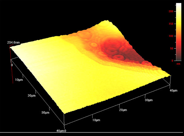
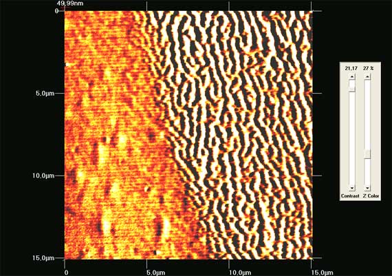
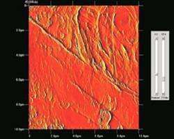
Image between exposed and non exposed areas of fluoropolymer at 157nm. Materials were provided by IMEL Demokritos. (zoom)
Surface morphology of exposed area of fluoropolymer at 157nm. Materials were provided by IMEL Demokritos. (zoom)
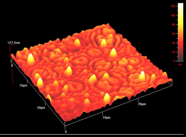
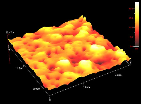
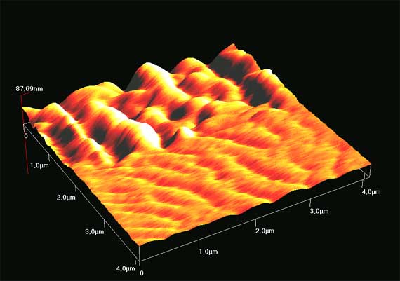
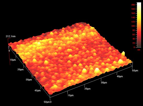
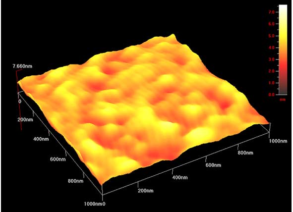
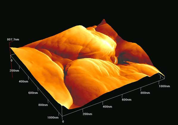
3D image of surface morphology of fluoropolymer. Materials were provided by IMEL Demokritos. (zoom)
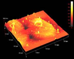
3D surface image of the exposed area of silicon based polymer at 157nm. Materials were provided by IMEL Demokritos. (zoom)
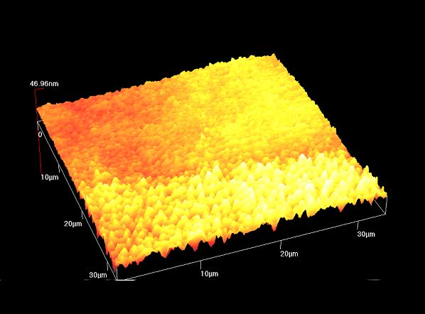
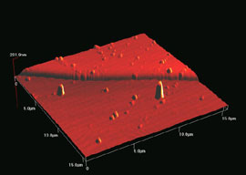
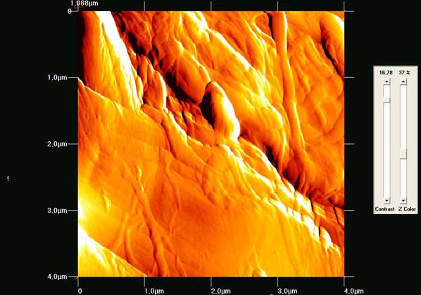
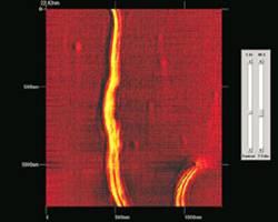
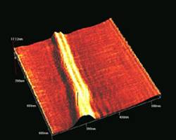
Image between exposed and non exposed areas of silicon based polymer at 157nm. Materials were provided by IMEL Demokritos. (zoom)
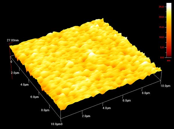
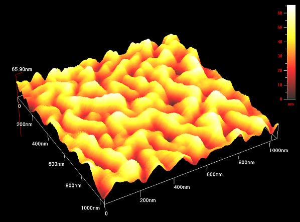
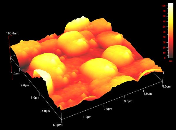
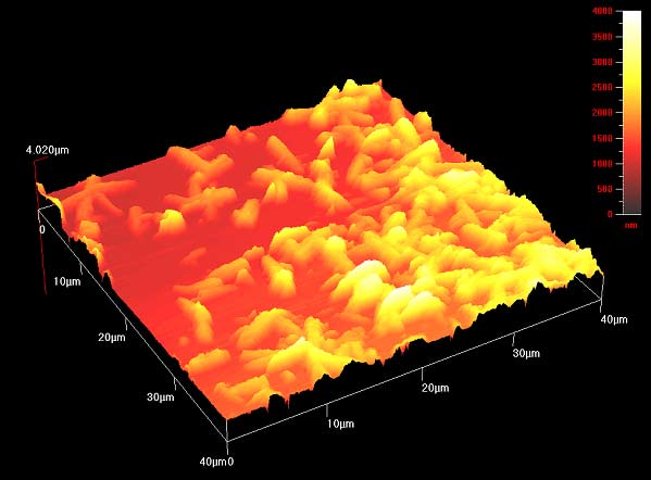
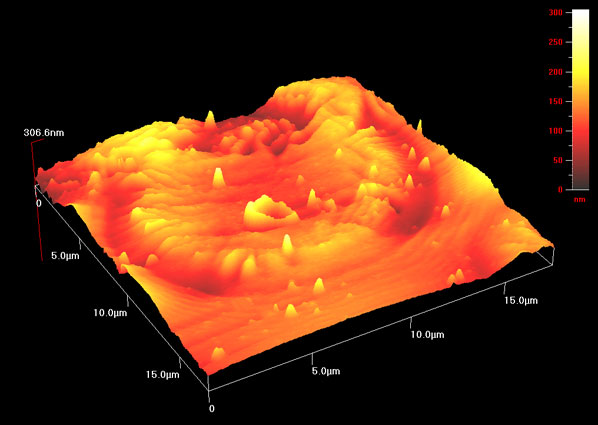
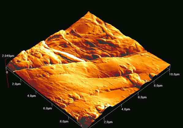
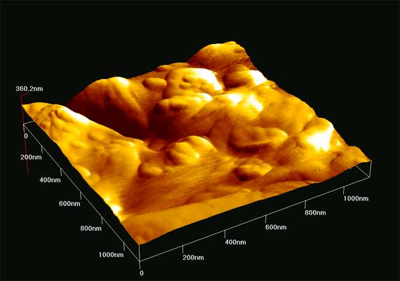
3D image of surface morphology of silicon based co-polymer. Materials were provided by IMEL Demokritos. (zoom)
3D image of surface morphology of silicon based co-polymer. Materials were provided by IMEL Demokritos.( zoom)
3D image of surface morphology of silicon based co-polymer. Materials were provided by IMEL Demokritos. ( zoom)
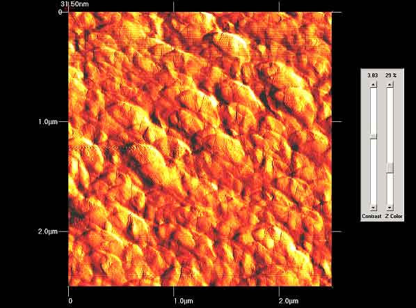
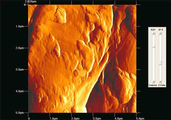
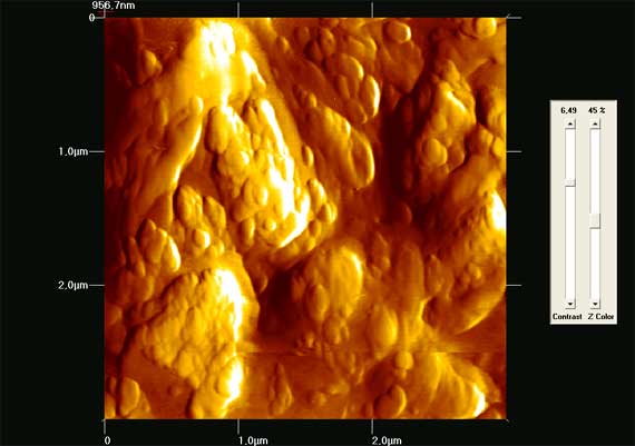
2D image of surface morphology of silicon based co-polymer. Materials were provided by IMEL Demokritos. ( zoom)
3D image between exposed and non exposed areas of Teflon film at 157nm. (zoom)
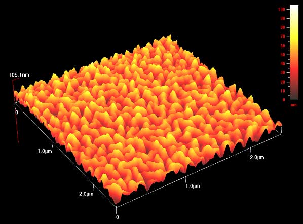
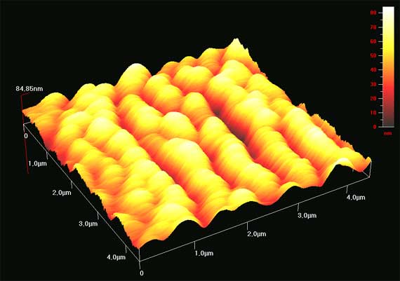
3D image of surface morphology of Teflon film . (zoom)
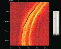
2D image between exposed and non exposed areas of Teflon film at 157nm. (zoom)
Metalic films
3D image of Si wafer coated with Ta layer using laser at 157nm. (zoom)
High resolution 3D image of Si wafer coated with Ta layer using laser at 157nm. (zoom)
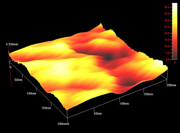
3D image of surface roughness of CaF 2 window. (zoom)
Quality evaluation of Au sputtered films. (zoom)
Biological
3D image of DNA crystals (Adenine). (zoom)
2D image of DNA crystals (Adenine). (zoom)
2D image of DNA crystals (Cytocine). (zoom)
3D image of DNA crystals (cytosine). The edge between the non-irradiated and radiated at 157nm areas is seen. (zoom)
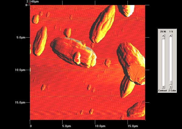
3D image of Ulocladium spore exposed at 157nm. (zoom)
Paper
2D image of non infected area of historic paper . (zoom)
2D image of non infected area of historic paper. (zoom)
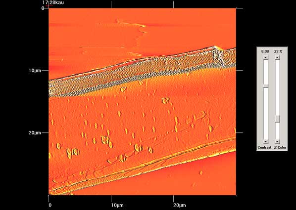
3D image of historic paper area. Infected by foxing area can be seen on the viewers side of the image. (zoom)
3D image of historic paper areas infected by foxing. (zoom)
2D image of historic paper area infected by foxing. (zoom)
2D phase mode image of historic paper. (zoom)
2D image of paper area. (zoom)
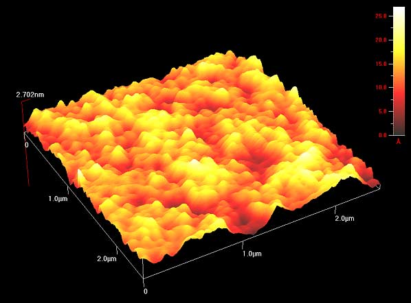
3D image of paper area. (zoom)
Carbon nanotubes
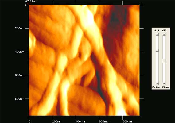
2D image of carbon nanotubes. Materials were provided by Dr. N. Tagmatarhis.(zoom)
3D image of carbon nanotubes. Materials were provided by Dr. N. Tagmatarhis. (zoom)
2D image of carbon nanotubes. Materials were provided by Dr. N. Tagmatarhis . (zoom)
