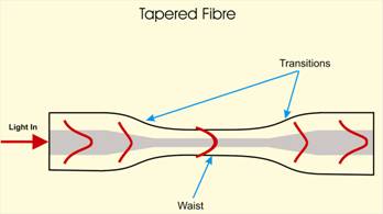
Silica nanofibres are made by stretching a heated conventional telecommunications fibre, forming a structure comprising a narrow stretched filament (the ''taper waist''), each end of which is linked to unstretched fibre by a conical tapered section (the ''taper transition''), as depicted in Fig. 1. Shrinking a single-mode core usually makes the mode expand not contract. If the outer diameter reduces further, the mode will soon expand enough to meet it, and then light is guided by
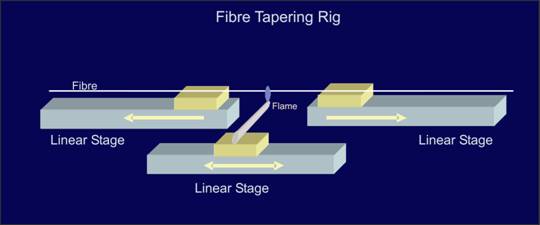
the glass-air boundary as a cladding mode. The entire fibre acts as a waveguide core and the surrounding air as its cladding, the residual fibre core having little effect. The reverse process occurs downstream: the mode withdraws from the outer boundary and is recaptured by the expanding fibre core. The (usually) large diameter and index step of the glass-air waveguide makes the nanofibre waveguide highly multimode, but as long as the transition is adiabatic the higher-order modes are not excited. The higher-order modes evolve from the cladding modes of the uncoated "single-mode" fibre. A flame tapering rig is used for the fabrication of the silica nanowires. Scanning the small (~2 mm for the flame) hot zone several mm to and fro along the fibre allows greater control of the resulting structure than a static heat source, giving a uniform waist diameter and taper transitions of controllable shape (see Fig.2). The rig is fully automatic capable to follow the exact design parameters and it can fabricate silica nanofibres with diameters down to 400 nm and with overall insertion loss less than 0.02 dB.
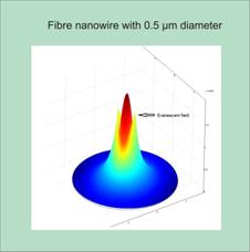
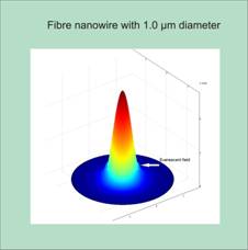
Light guided at the outer boundary of a taper waist can interact with external media via the evanescent field. This can be exploited for sensing. Parameters like the diameter and length of the uniform waist, the shape and length of the taper transitions, the bending of the waist, the surrounding refractive index can influence the performance of the silica nanowire sensors.
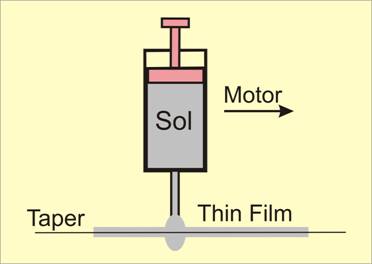
The thin silica nanofibre waveguides can be activated as active sensors using sol-gel technology. In a narrow waist of few micrometers diameter, the fundamental mode is guided as a cladding mode at the outer boundary, and can interact with external media (such as a porous sol-gel derived film) via the evanescent field. Samples of conventional fibre (Corning SMF-28) will be tapered to a uniform waist diameter specified. In a variant of the well-known dip-coating processes, Fig. 2, a droplet of sol suspended at the tip of a syringe needle will be passed along the taper waist, trailing a thin layer that will be gelled almost immediately on exposure to air. A small number such passes can form a very thin film of slightly porous silica glass.
Photonic Crystal Fibres
Photonic crystal fibres (PCFs) constitute a new kind of optical fibre proposed by Philip Russell in 1991. In contrast to conventional fibers, PCF is made by using just a single material, for example fused silica, and has a regular pattern of tiny air holes running along its length. When an air hole is replaced with solid glass, light can be guided by total internal reflection. The air holes have the effect of reducing the refractive index of the cladding region relative to the core. Confinement occurs because the encircling air holes act as a ''mode sieve'' blocking the fundamental mode whilst allowing higher-order modes with shorter effective transverse wavelengths to escape into the cladding. As a result, the guiding properties of the fiber are governed primarily by the size, shape and pitch of the air holes, and there is a certain air-filling fraction below which the fiber has no cut-off wavelength and is therefore endlessly single mode.
Endlessly Single Mode (ESM) PCF
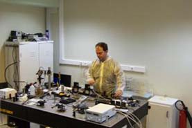
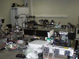
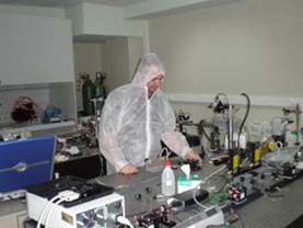
Photonics Lab
TPCI Staff
Researchers: G. Kakarantzas
Graduate Student: C. Markos
Collaborations
Photonic Networks and Technology Laboratory, Computer Engineering and Informatics Dept., University of Patras, Greece (K.Vlachos)
Depto. de Fisica Aplicada-ICMUV, Universidad de Valencia, Spain. (A. Diez)
Department of Mathematical Sciences, University of Technology, Sydney, Australia (C. Poulton).
Support
EDA JIP-ICET ''SESAMO''
ESPA 2007-2013 Synergasia GSRT ''MEDOUSA''
Contact
Dr. Georgios Kakarantzas
Associate Researcher
Photonics and Nano-applications Laboratory
Theoretical and Physical Chemistry Institute (TPCI)
National Hellenic Research Foundation (N.H.R.F)
48 Vassileos Constantinou Avenue
11635, Athens
Tel Office: +30 2107273843
Tel Lab: +30 2107273643
Fax: +30 2107273842
email: gkakaran
Web: http://www.eie.gr/nhrf/institutes/tpci/cvs/cv-kakaratzas-en.html